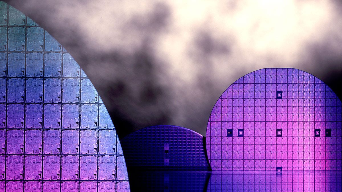
How to Accelerate Semiconductor Manufacturing
Semiconductors have helped move innovation forward, from advancing the first space travel to the first autonomous vehicle-they are a powerful technology. They are widely used in many products we use and depend on every day, from smartphones and computers to transportation and industrial manufacturing. Advances in semiconductors have touched every aspect of our lives and made them more convenient, safe, and productive.
The COVID-19 pandemic has fundamentally reshaped many aspects of the global economic order, affecting nearly every industry by disrupting supply chains and introducing near-term uncertainty in supply-demand cycles.
The semiconductor industry is no exemption; with the rising cost of innovation for semiconductor manufacturing and design, the industry continues to face both internal and external challenges. Externally, the cost of innovation climbs higher as investment expenditures steadily increase; internally, manufacturing remains a delicate and intricate process that requires a highly controlled environment.
Increased demand
Semiconductors also allow for the creation of new and emerging markets, such as artificial intelligence (AI), quantum computing, and advanced wireless networks, opening up new sources of demand. Trends like automation, electrification, and digital connectivity and security, along with other increased demands, forced the industry to evolve and use more advanced or modified silicon-type wafers.
Silicon carbide wafers, as an example, are used in optoelectronics, solar inverters, and industrial motor drives due to their thermal capabilities while silicon germanium and gallium arsenide are finding ways to advance applications in silicon-based lasers.
Evolving needs
Manufacturers and R&D facilities are constantly looking to improve processes by utilizing purer chemicals and reagents thus needing sensitive and reliable analytical testing solutions.
Equipment is required to provide low detection levels of critical impurities that seamlessly integrate with on-line sampling accessories for real-time monitoring to provide improved efficiencies and production uptime.
Testing obstacles
The major challenge in semiconductor wafer testing right now is around scale; the size of devices is becoming smaller and smaller, requiring instrumentation with increasingly improved detection limits. A small defect or contamination on a large device would not have such an adverse effect as the same defect on a much smaller device.
Manufacturing processes that have been satisfactory in the past for fabricating large devices may not be applicable to smaller devices and may lead to flaws. Materials used in the manufacturing and cleaning processes need to be of increasing purity. There are several cleaning processes involved from raw material to final products and each step has the possibility of either improving the cleanliness or introducing contamination into the process. Great care is required in the choice of materials and their application.
In addition, to move forward and to cope with the increased demand for devices the industry may need to move to alternative materials that will require a whole new suite of methods and possibly additional analytical techniques.
Defect and failure analysis
Wafer defect management challenges can be introduced at any stage of the manufacturing process, so testing at multiple stages is necessary, starting at the beginning of the process with the raw materials. Multiple analytical techniques can be deployed to determine elemental and organic composition as well as physical testing of the materials.
After the starting materials are introduced into the manufacturing process, there will be a wafer functionalization process where a functional surface combines the properties of the substrate and the functionalized group to produce a material that can combine aspects of each. Additionally, coatings may be applied to the wafers to assist with wafer processing or to achieve the required functionality for further processing. In each of these cases, the presence, content, and uniformity of the coatings need to be determined.
And finally, any residual impurities could have a negative impact on the performance of the wafer and/or the final manufactured device. So, control and detection of impurities are essential throughout the manufacturing process.
In terms of routine quality assurance / quality control (QA/QC) analyses, it is essential to have reliable instrumentation and software that is easy to use, can run standard methods, and be suitable for the environment it is to be used in.
For quality control and failure analysis, the instrumentation must be versatile and offer the highest performance to overcome a range of problems. Learn more about how the MappIR with Spectrum 3 FT-IR helps address and overcome these challenges: